
In response to this shifting landscape, manufacturers find themselves at the nexus of a transformative journey. The imperative is to produce electronics at a lower cost and achieve operational efficiency and agility. The multifaceted challenge encompasses streamlining manufacturing processes, trimming operational costs, and accelerating production cycles. This approach necessitates an intricate interplay of innovative methodologies and advanced technologies that optimises the in-circuit testing procedures needed for ensuring the quality and functionality of electronic products, as shown in Figure 1.
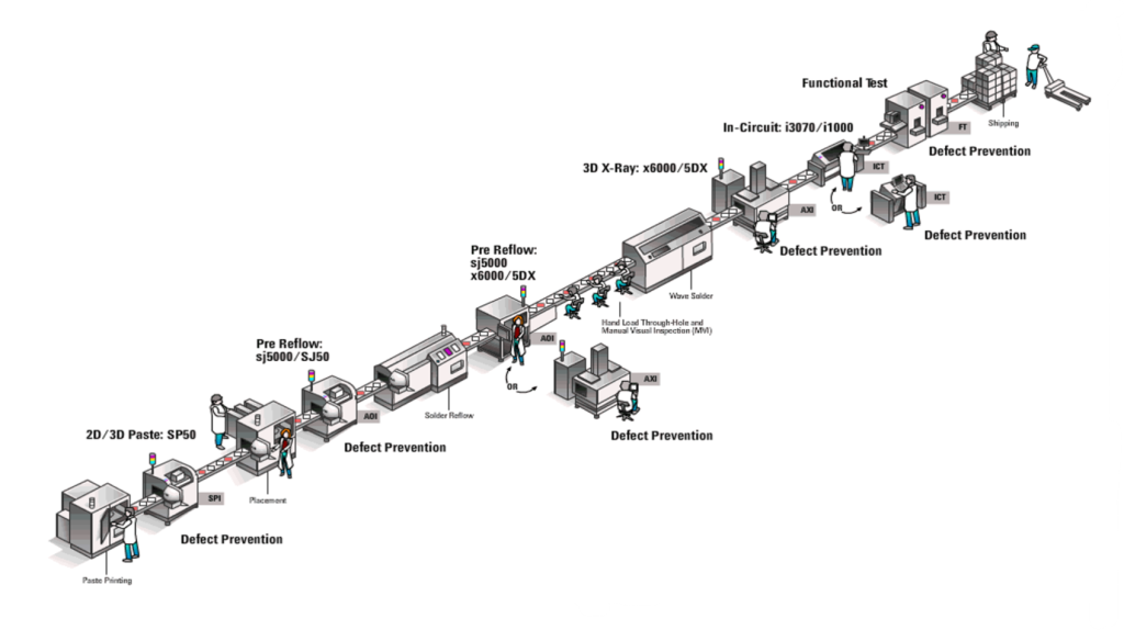
Figure 1. A typical production line with multiple test stations
Challenges in conventional test approaches
In recent years, there has been a significant increase in demand for high-volume production of low-complexity printed circuit boards (PCBs). As a result, manufacturing processes must streamlined by improving production times.
One key aspect of ensuring high-quality production hinges on the testing process, which is particularly crucial for boards that require regular testing stages and flash programming. The conventional testing protocol for such boards typically involves multiple test stations, encompassing in-circuit tests (ICTs), flash programming, and functional testing. However, this methodology is unsuitable for high-volume production due to its constraints on test throughput and the high costs associated with multiple test stations.
Navigating high-volume manufacturing: Industry approaches and solutions
One way to overcome testing challenges for high-volume manufacturing of low-complexity boards is to adopt the PCB panelisation manufacturing technique. Using highly panelised boards has become a common technique in manufacturing, improving throughput and increasing production volumes. Low-cost electronics are also usually smaller and lower in complexity, so multiples of these types of boards can fit into a panel of manageable size.
In PCB panelisation, manufacturers create one board from several boards and assemble them to form a single array. This technique involves fitting these smaller and less complex boards into a panel of manageable size, making it more cost-effective to move them through the assembly line.
The boards that make up the panel enable operators to load just one panel to test all boards simultaneously. During the breakout process following assembly, the panel divides into separate PCBs, a procedure known as depanelisation. The individual boards can be readily depanelised or separated from the array for packaging or installation into products.
Assembly of low-complexity boards in production is often rapid, necessitating quick turnaround times for testing to meet the production rate.
The following are examples of high-volume, low-complexity board devices across various industries:
- Automotive electronics, including sensor boards, controller boards, and engine control units (ECUs)
- Medical devices such as glucose metres, blood pressure monitors, and pulse oximeters
- IoT devices, including smart speakers, smart door locks, and home security systems
- Mobile devices such as smartphones, wearables, and tablets
Panelising PCBs not only assists smaller boards in conforming to standard production procedures, but also enhances production efficiency. Some advantages of PCB panelisation include saving time and money, improving work efficiency, enhancing product quality, and increasing output.
How does parallel panel testing improve testing efficiency?
A parallel test method enables testing multiple boards simultaneously. This approach of parallel panel testing facilitates in-circuit tests to meet high-volume production demands effectively (Table 1).
| Test method | Single board test time | Number of boards | Total test time |
| Sequential testing | 6 seconds | 20 | 120 seconds |
| Parallel testing | 6 seconds | 20 | 30 seconds |
Table 1. Sequential versus parallel test time
For example, if a single board takes six seconds to test, meeting the high-volume production demands necessitates a throughput of four boards every six seconds, totalling 2,400 boards per hour. Testing one board at a time per tester is insufficient to meet these requirements. To achieve the necessary throughput, the manufacturer faces two options:
- Purchase four testers, which would demand additional operators and floor space
- Invest in a single tester capable of testing all four boards in parallel
Testing four boards sequentially using one tester would require four times the single-board test time, totalling 16 seconds. However, testing four boards in parallel reduces the overall test time to approximately six seconds. This method represents a test time savings of 10 seconds over the testing of four boards sequentially.
Massively parallel testing — maximising test efficiency and reducing testing time
High-volume, low-complexity PCBA testing requires a test system that can conduct ICT, flash programming, and functional testing to keep up with high production volumes. Massively parallel board testing can test multiple boards at the same time using multiple testing cores.
In traditional setups, in-circuit testers typically limit testing to up to four boards simultaneously. However, in high-volume manufacturing scenarios, where efficiency and throughput are paramount, the demand rises for the ability to test a larger quantity of boards in parallel. In-circuit testers must be capable of testing 10 to 20 boards in parallel to meet these demands.
Given their simpler and smaller board designs, low-complexity products can accommodate 20 boards on a single manageable-sized panel. In-circuit testers capable of massively parallel testing are with test cores to execute tests for all boards in the panel in parallel. This approach integrates multiple testers into one unified system.
Furthermore, massively parallel testing can lead to an increase in the density of panel testing. Parallel tests a greater number of boards simultaneously on a single panel. Consequently, there is a reduction in the requirement for additional fixtures, test operators, and floor space, resulting in cost savings and enhanced production scalability. Overall, massively parallel testing provides advantages over standard parallel testing, especially in the realm of high-volume manufacturing.
Table 2 shows the benchmark conducted on individual boards, panels of four, and panels of six, demonstrating that throughput increases as the number of units on a panel grows. Parallel testing attributes this outcome to the simultaneous testing of multiple units, consequently reducing overall testing time.
Table 2. PCBA test time for sequential versus parallel test
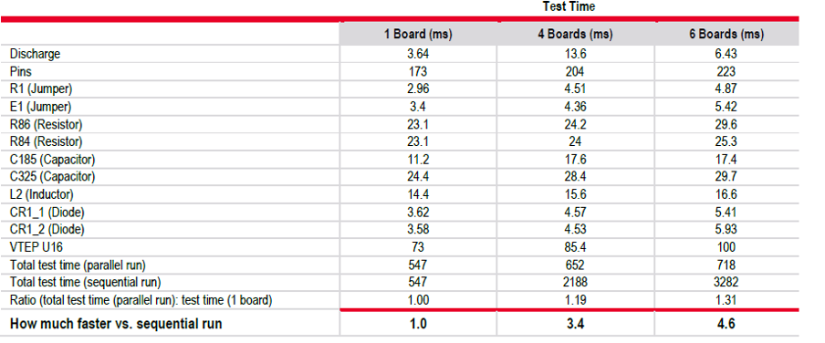
In contrast, sequential testing, which evaluates one unit at a time, inherently operates at a slower pace due to the necessity of finishing each test before initiating the next. This sequential approach leads to bottlenecks within the testing process, consequently impeding the overall testing rate. However, by implementing parallel testing, where we assess multiple units simultaneously, we reduce the time needed to test each unit. This advancement significantly boosts testing throughput and efficiency across the board, optimising the testing process.
Conclusion
To optimise the testing process for high-volume, low-complexity manufacturing of PCBs, a panelisation technique is employed alongside a parallel test system. This method facilitates the integration of smaller, less intricate boards into manageable panel sizes, enhancing cost-effectiveness while notably reducing loading and test times. Moreover, the implementation of massively parallel testing allows operators to simultaneously test multiple boards, ensuring swift test throughput, streamlined functional test measurements, and a cost-effective approach to overcoming the challenges associated with high-volume manufacturing of less complex boards. Massively parallel testing emerges as the quintessential solution for high-volume board test production environments, delivering prompt and dependable test results.

